New article on Point Defect Parameters of a 300 mm Czochralski Silicon Crystal
Our researchers Andrejs Sabanskis ![]() and Jānis Virbulis
and Jānis Virbulis ![]() have recently published an article Evaluation of the Performance of Published Point Defect Parameter Sets in Cone and Body Phase of a 300 mm Czochralski Silicon Crystal. The article was co-authored with Matīss Plāte, Andreas Sattler and Alfred Miller from a German company Siltronic AG; and it was published in the special issue Modelling of Crystal Growth of a peer-reviewed, open-access journal Crystals.
have recently published an article Evaluation of the Performance of Published Point Defect Parameter Sets in Cone and Body Phase of a 300 mm Czochralski Silicon Crystal. The article was co-authored with Matīss Plāte, Andreas Sattler and Alfred Miller from a German company Siltronic AG; and it was published in the special issue Modelling of Crystal Growth of a peer-reviewed, open-access journal Crystals.
Modern technology cannot be imagined without silicon microchips – they are embedded into everything from hospital beds and washing machines to computers, cars, planes, and space ships. The feature size of electronic devices is steadily decreasing. To have reliable electronic devices, it is of utmost importance to reduce the size and number of grown-in defects such as voids and agglomerates in silicon wafers.
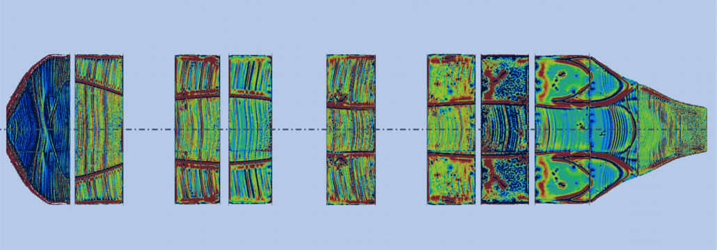
Simulating Czochralski silicon crystal growth is a widely applied technique for process development, e.g., for reducing the size and number of defects in Silicon wafers. In previous studies, several different sets of point defect parameters have been proposed. The published research article by A. Sabaniskis et. al. discusses the results of simulating the transient temperature, thermal stress and point defect distributions for 300 mm Czochralski growth of the whole crystal including cone and cylindrical growth phases. 12 different previously published point defect parameter sets were simulated, and the simulations were compared with experimental data – more specifically, experimentally measured interstitial–vacancy boundary. The results have been evaluated for standard and adjusted parameter sets. Considering the effect of the thermal stress on the equilibrium point defect concentration, the best agreement in the whole crystal was determined and is described in the article.
The article was published as part of the PostDoc project Effect of thermal stresses and growth conditions on the point defect and dislocation distributions in semiconductor crystals (1.1.1.2/VIAA/2/18/280).
The full article is openly accessible here.